
A few screenshots from my layout editing software. I wish there was a way to show more explicit shots, but this is not very easy. These are quite unreadable..
Tracks on the "solder" side (below) are in blue, on the component side (above) in red. Most of the component side surface is hogged by the ground plane though, so it only carries a few links and the pads for SMD components placed above. There are components on both sides, but we'll still call the the upper sidet the "component" side.
This is seen from above. Ground plane, has been made invisible. We see only parts placed on the coponent side.
This is the same image with some explanations overlaid.

The board, still seen from above, but this time with components going below. Notice the mirror effect...
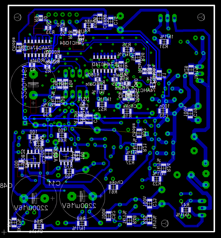
Finally a closeup on the digital circuitry, with ground plane enabled. I have also put a small ground plane on the solder side to act as a shield between tracks to minimize coupling (this is a technique used in low noise circuits to minimize charge bleeding). This ground plane has to be connected to the main ground plane by many closely spaced vias (these are all the seemingly useless little green spots). If not enough vias are used, the planes will oscillate with each other at HF.

Notice ultra-low profile sockets used for CS8412.


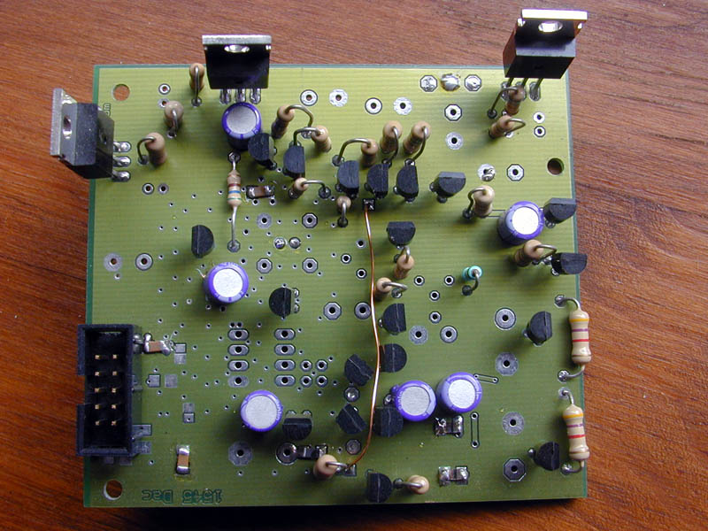

I could use a little cleaning fluid...

Tinned soft iron box at the left contains SPDIF modules and insulation transformers.
LM317 regulators have been relocated to the face plate for cooling.
A few corrections were made to the circuit (try to find them !)
The enameled copper wires carry the output to the lowpass filter, which is still breadboarded.
