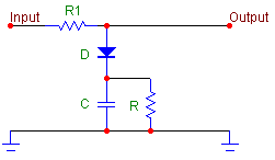
Fig.1 : the THD Trick
Copyright Advice : I first heard of this in a patent from a French designer named Gérard Perrot so Thanks to him. He owns intellectual property on some of the circuits. Fortunately this only concerns commercial matters and DIYers can't get sued from building stuff at home, even if it is patented by other people...
A French audio manufacturer, Lavardin, claimed the discovery of a previously neglected circuit characteristic, which they called "circuit memory". The root of phenomenon was, according to them, signal-induced thermal drifts in transistors. They developed an amplifier which supposedly eliminated this phenomenon.
Said amplifier got reviews to die for. Audio critics got hysterical. JM Lab uses it to power their Utopia line of loudspeaker in demos. However, the manufacturer in question being French, having limited production capacity, and expensive prices (although no so by audio standards), the scandal somehow faded as few people (not including me) could test listen the amplifier. Lavardin, however, seems to be doing good business.
When there's smoke there's fire.
It is not often that some claimed "discovery" in audio makes sense. I got a copy of the patents. They made sense. I'll try to sum up what I understood. I don't pretend to be the owner of the absolute truth. I do think, however, that I might attract your attention on a previously "neglected circuit characteristic", tickle your curiosity, and maybe interest you.
First, the obvious : circuit memory is the ability of a circuit to remember the past states of a signal. Here are some examples of memories :
I will not talk about inductors and capacitors directly, as integrating is part of their function. That's how filters are made.
Stored charges in junctions : this is a known problem, of which I am no specialist. They determine how long the amplifier takes to get out of clipping ; this is important because as long as the amplifier is in clipping, all signal is cut off. This is not of this kind of memory that we are going to talk about, however.
Check out this simple, bare circuit :
|
Fig.1 : the THD Trick |
Now imagine we measure its distortion, by sending a 1 KHz sine of constant amplitude at the input and connecting the output to an analyzer. With adequate component values, after a few seconds the cap is charged with the peak voltage of the sine wave minus a diode voltage. Once it is charged, almost no current flows in the diode anymore, and the sine wave passes untouched, giving very good distortion measurements.
If we were to listen to music through this, however, we would notice that, after several seconds of low amplitude signals, the cap has discharged and will completely clip the crescendo that follows. This circuit has memory : the cap voltage is an image of past amplitude peaks.
This example is rather extreme, but shows that measurements using constant amplitude signals will fail to describe a system that is used to reproduce signals with extremely wide dynamics !
Fig. 1-2 : Simplistic amplifier | Fig. 1-3 : Output voltage (inverted, upper curve) and derivative (lower curve) versus Input voltage |
Fig.2 shows the transfer function of this amplifier : a portion of exponential fading into a straight line as the emmiter degeneration resistor kicks in. This particular circuit is not very linear, as the gain curve shows (red curve in Fig. 1-3). We see clipping, also.
If we were to use this amplifier in real life, we would need to choose a DC bias point around which to operate. Let it be VInput=0.7V+AC. Now, we can re-center the transfer function curves around the DC bias point : Fig. 1-4 has the transfer function for an input signal of +/- 20 mV around the DC Bias.
I also stepped the DC Bias from 700mV to 750mV in 5mV steps : these are the series of curves on Fig. 1-4. Transfer function is still the blue one and gain (derivative) the red one.
Fig. 1-4 : Effect of DC Bias variation on transfer function |
Shifting the DC bias simply shifts the curves horizontally, their global shape does not change at all. However, the part of the curve that is used for amplification is the one at the center, therefore its shape changes with DC Bias.
Each of these transfer function has its own non-linearities, gains, and probably sonic character. It is safe to assume that if we built the circuit and measured its distortion, the harmonics spectra would be different between 700mV and 750mV biasses, and even between each 5 mV bias curve.
Besides, if we use this circuit in an amplifier with global feedback, which is typically done, its gain will be a part of the global open-loop gain. The open-loop gain will then be dependent on the DC bias of that transistor.
Executive summary : Every parameter of the transistor depends of its DC operating point (Bias) :
So, am I re-inventing intermodulation distortion, you will ask. For all intents and purposes all I wrote above in 3. is strictly a rehash of known stuff on intermodulation distortion (IMD). Besides, IMD is not a problem in a well designed, linear amplifier. So what ? Wait until you read the rest...
Consider the following simplified amplifier embryo (Fig. 1-5) : a diff pair (Q1 Q2) and a VAS (Q3). I put a PNP diff pair, a la Douglas Self, for a change.
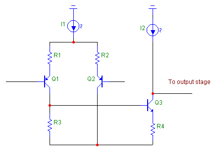
Fig. 1-5 : Some bits from an amplifier |
This makes for a high feedback design, with R1=R2=10R, R3=1K, R4=10R. Compensation cap is not drawn.
Let us do a thermal modelling of a realistic VAS transistor (Q3) : it will be a TO126 critter (BD139 as the usual suspect). Voltage-driven (like above), with I2=20mA and R4=10R. Typical values. The collector is loaded by a buffer transistor. Our thermal model is in Fig. 1-6 :
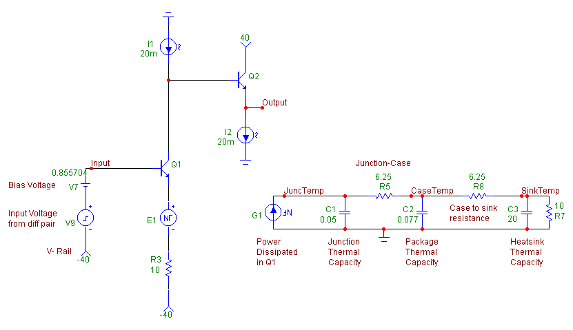
Fig. 1-6 : Thermal model |
Notice G1, a current source whose value is proportional to the power dissipated in Q1 (Vce*Ie), and the various caps and resistor that model the thermal capacitances and resistances of the transistor package and heatsink. Notice also E1, which models the Vbe variations of -2 mV/Celsius.
Now, let's drive it with a large transient signal, as shown in Fig. 1-7, which does not drive it into clipping, but close, and plot the temperature variations of the transistor silicon. This transient signal is 30V at the output for 20ms. The output voltage is in blue, the junction temperature in red :
Fig. 1-7a : Temperature variations on a large transient | Fig. 1-7b : Output voltage (zoomed) |
This transient heats Q1 by 0.215°C ; while this is very small, is is enough to create a noticeable variation of 1.37 V in the output voltage (Fig. 1-7b). This is because the very high input impedance of the buffer magnifies the minute current variations caused by the Vbe delta.
We can try other test signals :

Fig. 1-8a : Temperature variations on a 1 Hz tune | 
Fig. 1-8b : Temperature variations on a 10 Hz tune |
These output drift voltages will not appear at the output of the amp, as they will be corrected by global feedback. However, they will cause the DC bias of the whole amplifier to shift a little as the feedback corrects the DC error. The operating points of the input pair will change as well as the one of the VAS. As we have seen earlier, this will change the distortion spectrum of the amplifier, hence, its sonic character will be dependent on the power of the signal that has passed through it in the last seconds. It will not sound the same after a loud passage than after a quiet one ; powerful Bass notes will upset the balance too. It takes very little to upset an input pair, and Douglas Self measured that an imbalance as little as 1% in current between the two transistors is enough to generate a measurable increase in distortion.
As I wrote earlier, this could be considered like intermodulation, but it is intermodulation between the audio signal and the hidden variations of DC conditions. It is different from simple intermodulation between two frequencies, as this thermal drift signal can not be measured because the feedback corrects it. The drift signal also depends on the original signal, which makes it even worse.
Now, consider the model amplifier of Fig. 1-9. It has no output stage, and only the VAS transistor has a thermal model, to keep things simple.
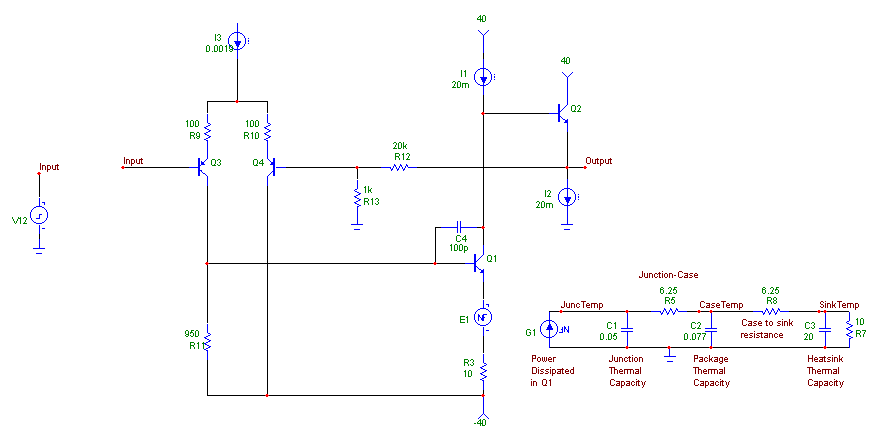
Fig. 1-9 : Simple model amplifier |
Having this amplifier process the large transient of Fig. 1-7 gives us the curves on Fig. 1-10 :
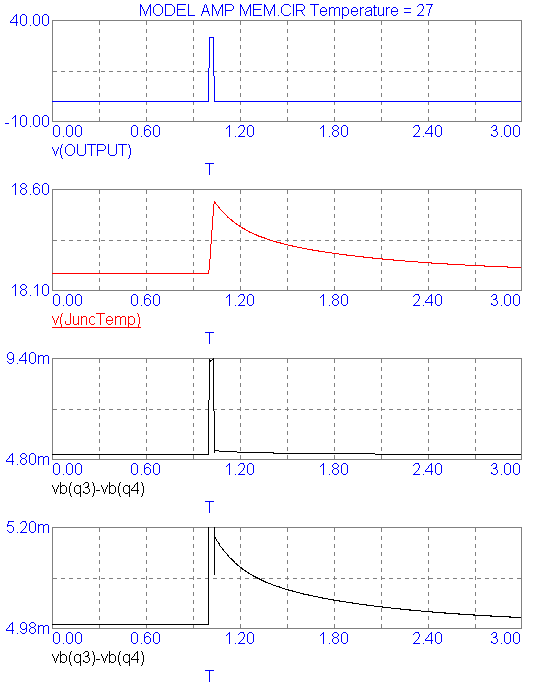
Fig. 1-10 : Thermal drifts in simple model amplifier |
Please note the amplifier is not driven into clipping. The temperature delta on Q1 is still there (red curve), but the output voltage (blue curve) shows only a measly 4 mV drift, instead of 1.37V : global feedback did its thing and nicely hides the gremlins from sight. We can still hear them scream, however.
The black curves show the drift of input pair error voltage Vb(Q3)-Vb(Q4) ; the bottom one is a closeup :
The thermal drifts therefore caused VError to shift of 197uV (this corresponds to the 1.37 value at the output if we multiply it by the OL gain). If we compare this to the VError during the impulse (4.322mV), we come to this shocking conclusion :
The thermal drift signal is only 27dB down from the musical signal !
Besides, if we neglect the base current of the buffer transistor Q2 (which is perfectly rational), Intensity in Q1 is constant and dissipated power varies linearly with signal amplitude. Therefore, Q1 thermal drifts are proportional with music signal amplitude, which comes to another bad thought :
This 27dB ratio does not depend on the signal amplitude ! but only on circuit design. It will affect the sound quality of the circuit at all levels.
Feedback hides the bias variations : as one stage gets imbalanced, the other stages will tend to get imbalanced too, but the opposite way, in a desperate effort to compensate.
We saw above that the thermal drifts of the VAS transistor were multiplied by its gain. Reducing the open-loop gain (by loading the VAS collector to ground with a resistor) therefore reduces the drifts, but it also reduces the feedback factor available to correct them, resulting in a draw. Besides, it adds distortion.
[Flame suit on] I personnally think that high feedback is preferable. TIM seems more like a legend to me. High feedback can be used more efficiently against memory effects. Besides, you can make a fast amp that has high feedback too. There will be more on this in the next article, which will cover the details of the amplifier I designed against memory distortion. [Flame suit off]
All files ate zipped. Images are in TIFF CCITT4 Format, which allows for excellent compression ratios (1/4 the size of Gif's). You can read them with ACDSee, Photoshop, Paint Shop Pro, and the like.
I was into electronics since a long time, but mostly digital. I had no idea how an audio amplifier worked until september, 2000 (!). If you want to know how I designed a small amplifier that looks impossible on paper, yet makes my reviewer-recommended, purist, prized-by-La nouvelle revue du son, $800 store-bought mosfet amp sound like a pocket AM radio, don't miss the next article !!!