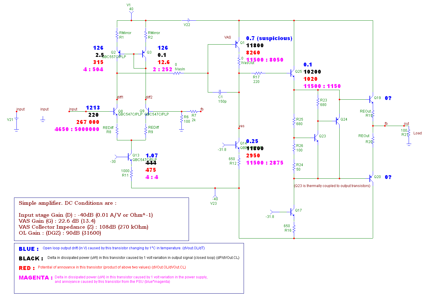
I was trying to figure out which transistors of the whole amp had the most influence on the total memory distortion. Then, the answer struck me as obvious : let's calculate the following two values :
In open-loop, the amp is very sensitive, so we can measure F = dV(Output Open Loop)/d(Temp), the variation of open-loop output voltage caused by a 1° variation in the tempearture of a specific transistor. F is in Volts/°C.
Therefore, for each transistor, we know
The product of these two values : A = H*F therefore gives an idea of how Annoying this transistor will be relative to the thermal drifts of the whole amplifier.
click to display schematic (hint : use shift-click)
Sorry for the huge graphics (I always work at 1600x1200). If you use Opera, hit "-" to zoom out. If you use an imperialist browser made by a monopolistic cartel, or a product of a defunct company, hit ctrl-alt-del.
Well well well, this is a standard sand amp, 90 dB open loop gain, 24 dB gain, 66 dB feedback at DC. Close to each transistor, I wrote the corresponding H, F, and A.
Now it is pretty obvious that the most annoying transistor is in the input pair, with some help from the VAS and its current sink.
The numbers for H are pretty logical, just think that Power=Voltage*Current and try to explain them.
The numbers for F get worse the closer you get to the input, because they are magnified by the gain of the rest of the amp. ie. a drift occuring in Q25 will not be multiplied by anything, whereas a drift occuring in the input pair will be multiplied by the full OL gain.
In Magenta, I wrote the results for the same technique applied to the power supply. Let's call H' the power variation caused by a 1 volt variation in supply voltage : d(Power)/d(Supply). Then, A'=H*F' relates to the sensitivity of the concerned transistor versus the power supply. The two numbers in magenta are H' : A'.
We can see the input stage is extremely sensitive to power supply variations.
As a side note, the thermal effects in both transistors of the input pair cancel each other, but not completely. The sore spot is therefore not only in the input stage, but also in the VAS and the current sources.
click to display schematic (hint : use shift-click)
The steps taken to operate critical transistors at constant power make the input stage almost imune to drifts : its annoyance factor dropped dramatically, both relative to signal (red) and to the power supply (magenta).
The current sources also benefitted a lot from cascoding. Same for the VAS.
We can see where the new sore spot is, and where to direct the efforts :
A major interest of this method is that the buffer transistor is shown to be quite innocent, where I would have thought the contrary.
Maybe this thing is going to get finished one day ?
All in all, the compensated amp sounds good (euphemish). 94dB feedback, why not ? I have no preconceptions on that.