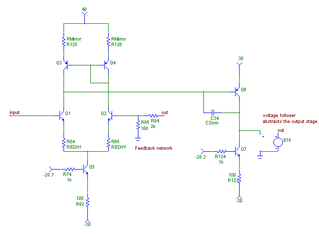
Fig. 3-1 : Our basic test circuits
The method that Gérard Perrot, author of the patents, used is very clever. The drifts we want to measure are hidden by feedback : as one stage gets imbalanced, the other stages will tend to get imbalanced too, but the opposite way, in a desperate effort to compensate. This must result in an extremely small drift voltage at the amplifier output, which is dependent on the actual internal drift, but much smaller. In order to detect it, integration of this offset over a period of time is used, as explained in the AES article that you can download by following this link.
Using the method described in the article, I simulated a number of circuits and their memory measurements. The test waveform was to make the amp output 20V during one second, and the thermal models used were pessimistic, to exacerbate memory effects and ease the search for a memory-free circuit topology. I started with the circuit of Fig. 3-4, and attached a thermal model to all transistors.

Fig. 3-1 : Our basic test circuits |
The resistors in the current sources are 100 Ohms, and the other circuit values are :
| ReDiff | 100 Ohms |
| RMirror | 100 Ohms |
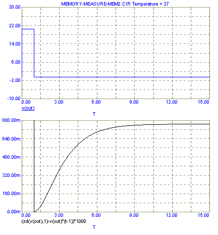
I will elaborate on the first measurement of Fig. 3-5 : you will see more of these strange-looking curves. This curve is simply the integration (sum over time) of the output offset voltage. Integration starts right after the end of the test waveform (we don't want to measure the waveform itself, but the memory of it). Once the test waveform is over (at t=1s), the output should return to zero volt. It doesn't however, because the bias points have shifted. Instead, the output voltage of the amp slowly comes back to normal as the transistors come back to their usual temperature. Integration shows us the total error summed over time, and this is a practical tool for evaluating the total memory of the amp.
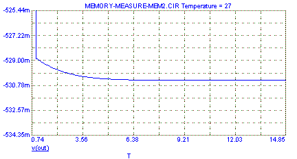
This gives us the curves in Fig. 3-2 : blue is output voltage, black is integrated memory signal. We can see the tiny variations of the output voltage in the zoomed curve on the right. Remember, these seem very small because they are hidden by feedback.

Fig. 3-2a : Memory, input stage only |

Fig. 3-2b : Output voltage, zoomed |
We will use the value the curve reaches at the far right (here 2.66) as a measurement of memory. These are arbitrary units, so the only use of such a value is for comparison. So, I will activate the thermal models in all the stages of the amp and plot their respective memories. I will not include all the curves here (they all look the same), but only their final values.
Of notable importance is, also, that I used the VAS transistor as a Current amplifier, whereas in article 1 it was used as a Voltage amplifier. In the voltage amplifier configuration, with resistors instead of the current mirror, Q6 generates much more memory, because the thermal Vbe errors are multiplied by the VAS gain, which is large. This gives memory measurements an order of magnitude higher than with the current mirror. Q6 Beta varies with temperature, also, but apparently this is much less problematic. It seems we will stick with the current mirror, then.
| Thermal model activated in... | Memory |
| None. | 0.00001 (roundoff errors) |
| Input pair (Q1,Q2) | 0.77 |
| Current mirror (Q3,Q4) | 0.27 |
| Tail current source (Q5) | 0.3 |
| VAS (Q6) | 4.76 |
| VAS Current source (Q7) | 2.7 |
| Both current sources | 3. |
| All at once | 4.83 |
Apparently we were a little bit over optimistic in part 2 by saying that the input stage would not really create offset on its own. It does, and quite happily, even if it is not the main source. These "almost negligible" values might not have been so negligible after all...
We will now apply the thermal models to all transistors except one stage, to see in which stages eliminating memory will benefit the most.
| Thermal model activated everywhere except in... | Memory | Gain |
| Input pair (Q1,Q2) | 3.08 | 1.75 |
| Current mirror (Q3,Q4) | 10.6 | Ouch ! |
| Tail current source (Q5) | 3.72 | 1.11 |
| VAS (Q6) | 0.63 | 4.2 |
| VAS Current source (Q7) | 3.86 | 0.97 |
| Both current sources | 2.68 | 2.17 |
The Current mirror looks suspicious ! There must be an interaction between this and other stages which partly cancels with all thermal models on, but deactivating the thermal model in the current mirror prevents this cancellation and gives strange measurements. I guess the only solution will be to optimize all parts of the circuit regarding memory.
In the next chapter, we will examine each of these circuit elements and see how we can get rid of their memory by adapting their topology.