A DAC board contains signals in a very large frequency spectrum. Square signals have harmonics all over ; and all this is modulated by digital audio data. Opportunities for noise pollution are all over the map.
I have to admit that I am not a specialist in RF/EMI compatibility and interference. This is a very large and complex discipline. Thus I cannot solve all problems. This forced me to adopt a simple philosophy : Try to suppress problems rather than try to solve them later.
I must say a big thank you to Mr. Guido Tent for all the invaluable information he gave in his documents, and some personal email exchange.
Meditate this often forgotten truth : Current travels in loops. There is always a return path. And there are many unofficial currents, because everything acts as a receiving antenna. A ground plane will not fix a badly designed circuit, but it helps a lot. However, a ground plane has to be well designed, which fortunately is pretty simple.
Very often we see DACs designed with split ground planes : an analog and a digital one, both ground planes being connected just under the DAC chip. This is a very bad idea and has earned its place in the Design Errors Hall of Shame. A split ground plane makes sure that many return currents travelling in the ground plane will have to go a long way around the split in order to close their loop. All these currents will run in the only possible place : right under the DAC (argh).
By making the ground plane uninterrupted, we trust Nature to help the electrons find their way. And these are not stupid : if they can, they will mostly travel the shortest, least annoying path, which is precisely what we want. A track on the solder side automatically becomes a transmission line if there is a ground plane on the other side of the board. At high frequencies, the return path will follow thsi track, minimizing noise emissions.
The complexity of any problem is exponential to the number of variables. Therefore we must reduce the number of variables. Here, these variables are all the loops interacting with each other. Just placing the components on the board and routing them is not enough.
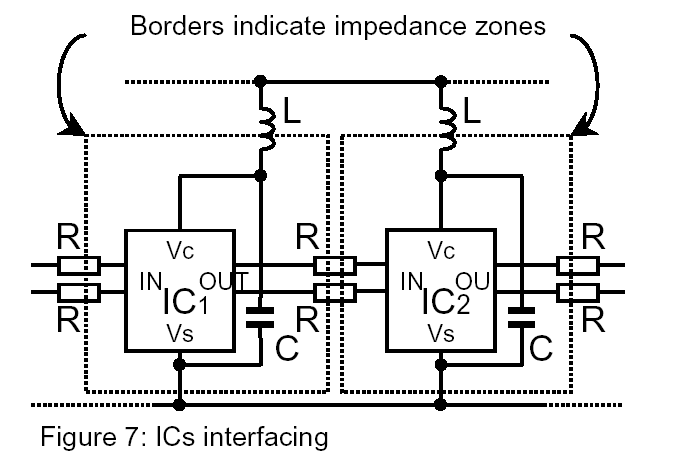
I will try to group parts into small groups which form meaningful functional units (for instance, clock unit, reclocking unit, buffer unit, etc.) and minimize interactions between units. These are called "impedance zones" because we try to maintain high impedance and low coupling between each zone. I prefer to call them Cubicles.
See an example on the figure below :
Here, we have two ICs performing different functions, which communicate via two signals.
This chapter was a very quick sum-up of this very rich document by Mr. Guido Tent which explans it all a lot better than myself. Required reading.
I designed a very elaborate supply system fot this dac. It is nonetheless very simple to understand.
The mains transformer, bridge, and caps are big noise generators. They live in a separate box.
I started with a surplus IEC connector with line filter. I chose a low bandwidth type transformer (not a toroid), to prevent mains noise from entering the circuit. Rectifiers are low noise diodes. The snubber is not placed around each diode, but rather across the transformer secondary, which is IMHO better. Read this article for more info. Reservoir caps are cheap, no-name type.
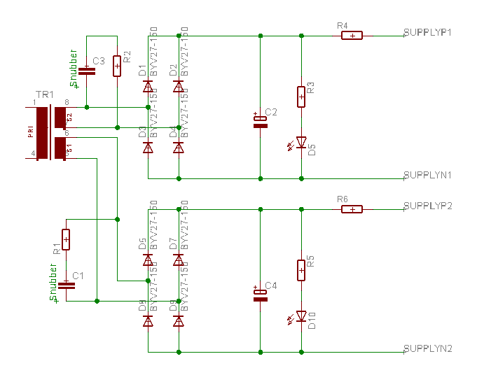
Now, the DAC supply current, which is quite constant, will travel to the DAC itself in a cable. Resistors (R4,R6) limit the 100 Hz current inrush to the small caps which do a little decoupling inside the DAC.
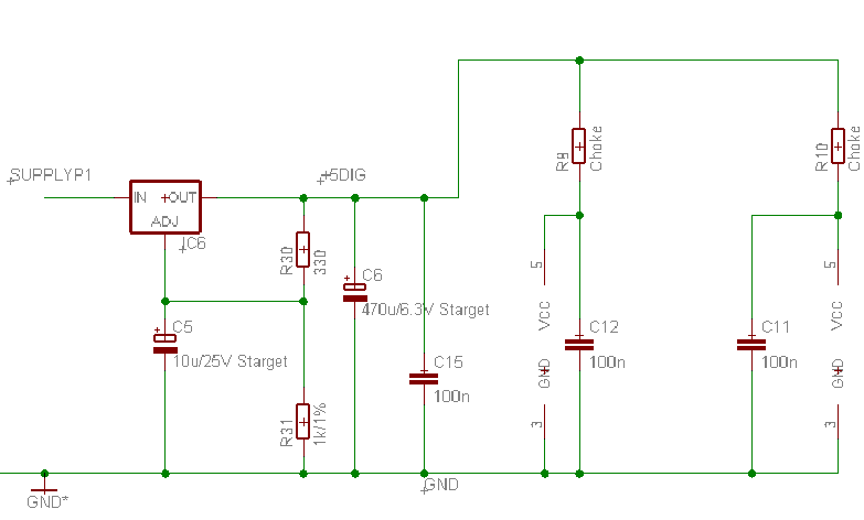
This is really a simple, LM317 regulated decoupled supply with a ferrite bead for each digital circuit (not all of them are represented on the schematic below). This supply is used for non-critical digital circuits :
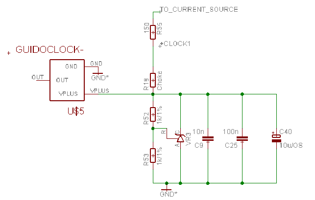
Every critical cubicle has its own powersupply : a low noise shunt-regulator (TL431) decoupled by an OSCON cap + 100n ceramic (credits: Thorsten Loesch). This gives a flat supply impedance from DC to tens of MHz. Lossy ceramic prevents ringing. Each of these shunt regulated supplies is fed from its own constant current sources through a choke.
OSCON caps are really wonderful. Cheap, extremely good performance all over the spectrum. Heartily recommended.
Look at the schematic below, showing us a shuntreg fed by a resistor (left) and by a current source (right).
Shuntregs are usually fed from a resistor. In that case, noise rejection is equal to the ratio of the resistance to the impedance of the shuntreg/cap combo. This is not a Good Thing, as we are often tempted to reduce the value of this resistance in order to lower total supply voltage requirements. On the other hand, a current source has a very high output impedance, giving much more noise rejection than a simple resistor. This is why I feed my shuntregs from current sources.
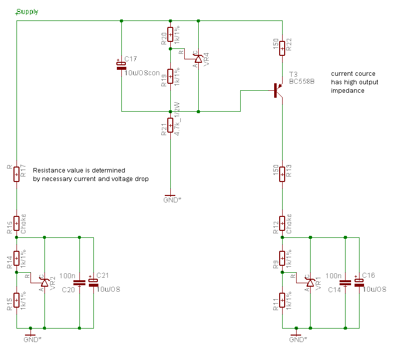
All current source share the same reference voltage, so this adds only one transistor and one resistor per individual supply, which is quite acceptable. Besides, the line between current source and regulator can be quite long without any RF problems because it carries constant current. The cost of each of these powersupplies is rather low both in terms of money and board space, if using SMD parts.
All these shuntregs are fed from a voltage regulated rail (LM317) and current sources sharing their voltage references. Not all current sources are represented on the schematic below :
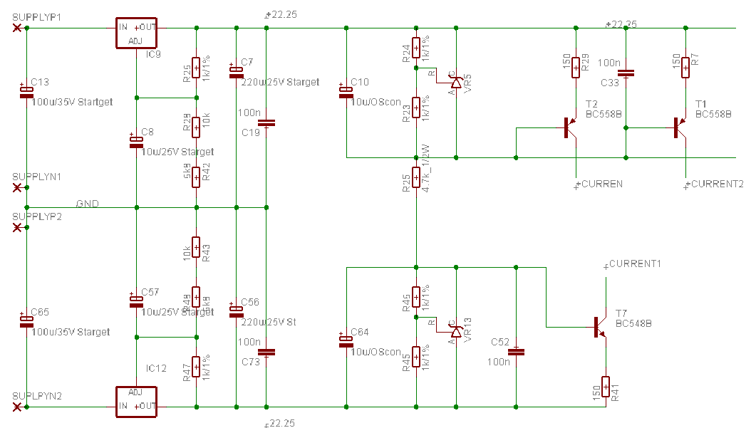
Taking the clock as an example, the only supply components which have to be located close to the clock are the regulator, its two resistors, decoupling caps and ferrite choke :