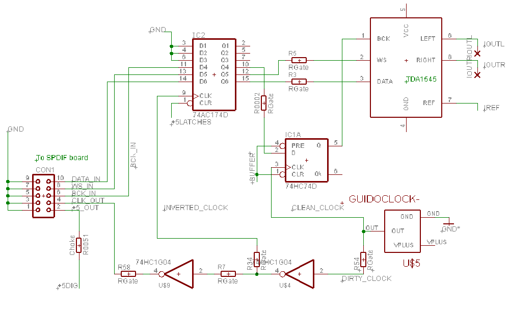
This schematic shows my reclocking unit :
The connector at the left leads to the SPDIF board, which needs a powersupply and clock signal, and provides I2S data : Bit Clock (BCK), Word Clock (WC) and Data. The connector is wired so a ground wire is present between every other wire.
The time-critical signal for the TDA1545A si BCK (it is the signal the chip uses to time its sampled output), and this is the one we must reclock most carefully. Other signals are not critical, the only condition for them is that they do not interfere with BCK.
I will start to describe this circuit from the clock itself (lower right). The clock signal directly feeds a latch (IC1A) which reclocks BCK just before it enters the DAC chip. This is to ensure lowest possible jitter, as BCK is the time ctitical signal. This clock signal is labeled "clean clock" as it is the raw signal from the clock itself.
Now, the clock can't feed many logic circuits, thus we send it to an inverting buffer (U$4) via a resistor (R54) to limit slew rate. This is labeled "Dirty clock" as we have limited its slew rate because it does not need to be precise : we have already taken care of BCK which is the only signal which needs precision. Notice the two slew limiting resistors R7 and R34. This inverted clock is sent to IC2 which is a 6-way latch out of which we only use 3 latches to reclock the three incoming signals.
Another inverter (U$9) buffers the clock to the SPDIF modulen, again with a resistor to limit RF emission from the cable between the two modules.
Now, you might ask, why this mess with inverted clocks ?
Consider the inverted clock. When it triggers IC2, new DATA/BCK/WC signals appear at IC2's outputs. DATA and WC go straight to the DAC. Thus, the instant when IC2 triggers is not a good moment to have BCK's time-crtical edge arriving at the DAC because DATA and WC are already making noise with their edges (remember the DATA signal is random). So, we make BCK wait a little in IC1A until a half clock has passed, and the mess has settled, before we send it to the DAC itself.
Besides, the WB/DATA/BCK lines coming from the SPDIF boards are noisy and should not be fed to a critical chip such as IC1A. They should either pass through a simple buffer, or be reclocked, as is the case here. Otherwise, noise picked up by these lines will influence IC1A and introduce jitter.
I think this reclocker is pretty good for so few circuits. All logic is SMD, and the inverters are PicoGates which are extremely small, to minimize loop areas. Decoupling caps are positioned on the other side of the board, just above the circuits, again to minimize loop areas.
This image shows how the critical clock path was laid out. Clock, IC1, IC2 are labeled in Red. The DAC is the DIL8 chip lower-left. Clock path is in Red. Ground plane and DAC powersupply is erased for the sake of readability, but other PSUs are visible.

The transport interface was relocated to another board for ease of future modification, and noise immunity. The schematic is very straightforward and should require no extra explaination :

Transport Interface Schematic
The "config" section is made of solder bridges which can be soldered (or not) to put the CS8412 in whichever mode we want.
LEDs display error information, generally indicating a bad SPDIF connection, and help for debugging. I have included a monostable for turning on the Error LED for a long time should a bit error be detected by the internal CRC checking. To date, this LED has never lit unless the SPDIF cable had a problem (like, being unplugged or something).
Here is the layout :

Transport Interface Layout
I made (myself) some insulation transformers for my Clock and SPDIF signals. I am afraid the details were lost. I will add more information here if I open the DAC again to count the turns...